Scanning Electron Microscopy (SEM)
See what’s really going on, right down to the microscopic level
Do you have something unexpected in your material, product, or sample?
We can tell you exactly what it is, where it came from, and what it’s made of even if you’ve never heard of SEM before.
You don’t need to know what SEM stands for to benefit from it. Here’s what our customers typically bring to us.
We identify the contaminant, its elemental make-up, and compare against a clean control sample to pinpoint the source.
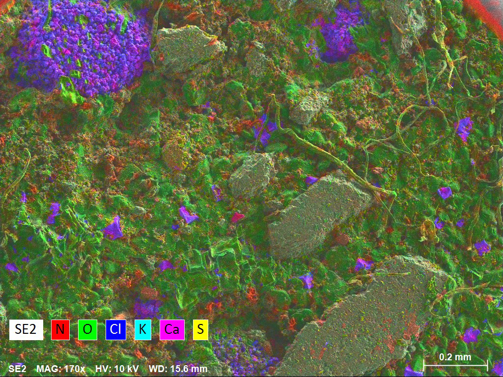
We produce detailed images and elemental maps of unknown samples — useful for quality control, R&D, and regulatory purposes.
We analyse scale deposits at the micron level — essential for understanding the chemistry of produced waters and planning treatment.
SEM/EDS identifies corrosion, damage, and chemical changes at a surface level. Ideal for engineering and failure analysis.
You send us the sample. We handle the science. You get clear, actionable results.
Solid samples, particles, or solids extracted from fluid in fact almost anything solid works. Tiny amounts are fine (even a few grains).
Using Carl Zeiss SEM with Bruker EDS detectors, we produce high-resolution images and detailed elemental maps of your sample.
What we found, what it means for your situation, and possible next steps.
| Minimum sample needed | Maximum solid size | Sample types | Technique |
| a few grains | ~5–8 cm² | Any solid material | Non-destructive |
Our SEM/EDS service supports a wide range of sectors. Select your area to see how we can help.
SEM/EDS has a strong track record in oil and gas particularly in understanding what’s forming in pipelines and produced water systems, and why treatments are or aren’t working.
- Analysis of scale deposits from produced water systems
- Corrosion investigation — identifying chemical and physical changes to materials
- Formation damage characterisation using standard and cryogenic SEM methods
- Comparison of treated vs untreated samples to evaluate treatment effectiveness
SEM examples from our lab
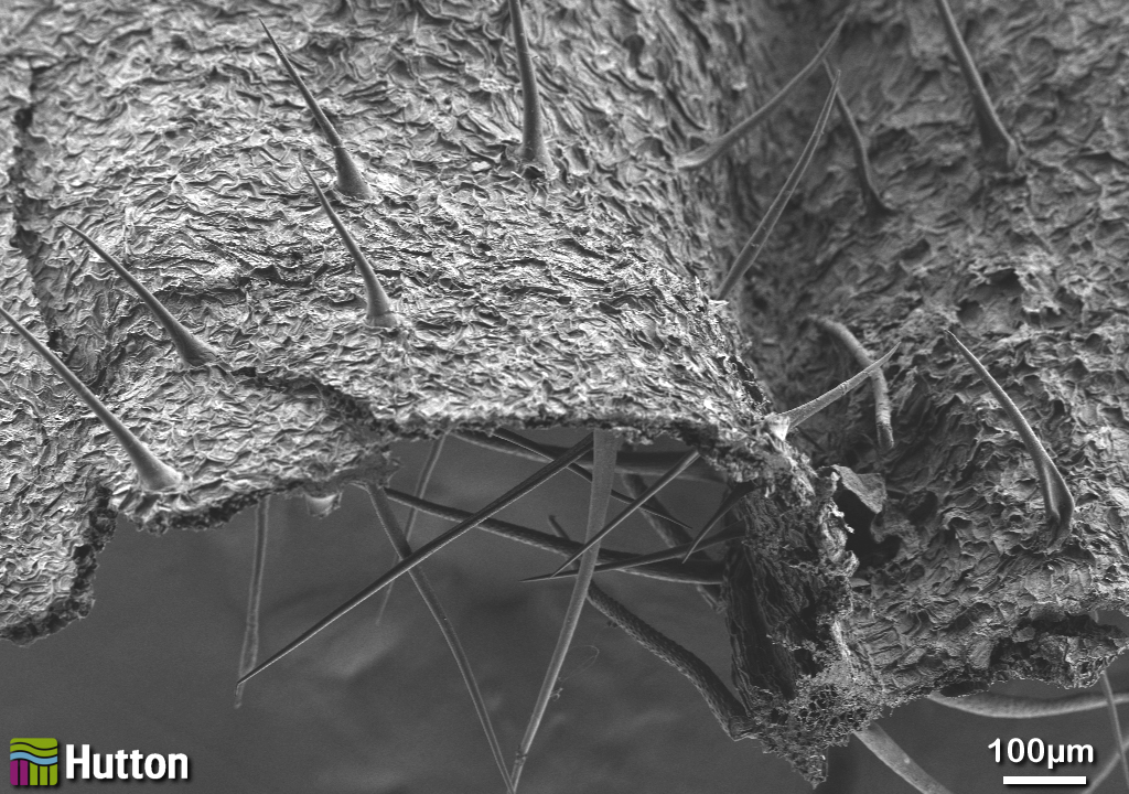
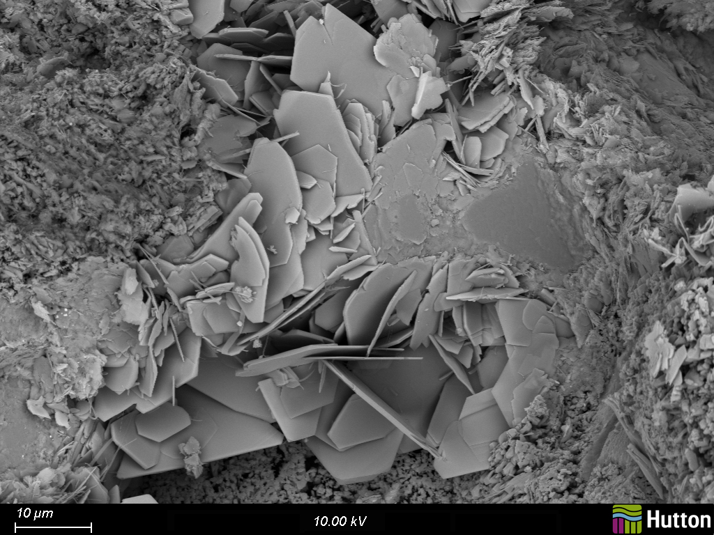
Scanning Electron Microscopy (SEM) is an advanced imaging technique used to examine the surface structure and composition of materials at very high magnification. James Hutton Institute Scientific Services uses SEM to produce detailed images and elemental analysis of samples, supporting research across environmental science, geology, agriculture and materials science.
Absolutely — that’s one of the most common reasons people come to us. SEM gives us a detailed image of your sample’s surface, while EDS identifies the elements it contains. Between the two, we can usually tell you a great deal about an unknown material: its structure, composition, and in many cases its likely origin or source.
Very little — even a few grains is enough for analysis. For larger solid pieces, our chamber accommodates samples up to approximately 5–8 cm². If you have a fluid sample with solids in suspension, we can extract and dry the solids prior to analysis. Not sure if your sample is suitable? Just drop us an email and we’ll advise.
No. SEM/EDS is a non-destructive technique, meaning your sample remains intact throughout the process. Once analysis is complete, we can return it to you or pass it on for additional testing just let us know your preference when you get in touch.
Turnaround time depends on sample complexity and current demand, but most analyses are completed within five working days of receiving your sample. If you have an urgent requirement, get in touch and we’ll do our best to accommodate you.
SEM (Scanning Electron Microscopy) produces high-resolution images of a sample’s surface — revealing structure, shape, and texture at a microscopic level. EDS (Energy Dispersive Spectroscopy) tells us the elemental composition — essentially what the material is made of. In most cases, running both together gives you the most complete picture. We’ll advise on the right approach for your specific sample and question.
Contact for more information
Laura-Jane Strachan
Head of Electron Microscopy
Based in Aberdeen
Laura-Jane Strachan gained a degree in Geology and an honors degree in Geography from the University of Aberdeen. She came to the James Hutton Institute in 2011 with over 5 years experience of working in the oil and gas industry. Her previous experience is in the identification of solid and fluid induced mechanisms causing formation damage, using standard and cryogenic SEM methods and thin section analysis
Laura-Jane currently works in the Electron Microscopy section and predominantly works on commercial projects, using Scanning Electron Microscopy to characterise a range of sample types.